WORKING WITH:
kiCAD
- kiCAD is an ‘Open Source Electronics Design Automation Suite’
useful resource for PCB terminology
DEFINITIONS:
FOOTPRINT
- :defines the copper connections between physical components and the routed traces on a circuit board
- the physical interface between each electronical component and the printed circuit board
TRACK
: a conductive path that is used to connect 2 points in the PCB
PAD
- : a small surface of copper in a printed circuit board that allows soldering the component to the board
- two types; thru-hole and SMD (surface mount)
NET
: collection of pads on the PCB that should be electrically connected to one another
STEPS
-
once you make a file, the sch file is your circuit editor
-
using the third icon in the right toolbar, you can add new components/symbols for components
-
arrange them into their according structure
-
connect them one by one using wire (the white/green straight line in the right toolbar)
- assign values to components
- click on a component and hit key e (or double left click)
-
generate netlist (happens automatically during next step so disregard)
- go to assigning PCD footprints to schematic symbols (footprint assignment tool in top toolbar button)
THE POP-UP WINDOW: in the left column are the categories in the center column are the components you used in your circuit diagram in the right column are the individual components
-
In the center, select the first of your components
-
In the left, find the category in which it fits
-
In the right, select one of the components within that category
-
In the top left toolbar, you can check if this selected component suits your component by ‘viewing the selected footprint in footprint viewer’
-
If it looks good to you, close the footprint viewer and double click on that component in the right column so it becomes visible in the center as well
-
Do this for all your components
-
press the button in the bottom right apply, save schematic and continue
-
click okay
-
after these steps, you can now go to PCB editor view
-
Update PCB view from schematic
-
in this pop-up window, click on update PCB
-
place the PCB by clicking on an area in the PCB view
-
We now need to arrange the components on the board
- the shortcuts are the same as in the schematic editor
-
You can then start routing
- first we change a couple of design rules: decide which track to use and what copper (B.Cu PgUp)
- select the routing tool in the right toolbar
- if a track is overlapping, you can either: choose the other side of the copper (F.Cu PgDn) for that track wire method: use B.Cu PgUp and when it is about to overlap you right click and select place through via
-
We now make the edge cuts
- choose edge cuts in the top right (where you selected the copper)
- select add graphic lines
- make the outline of your circuit board
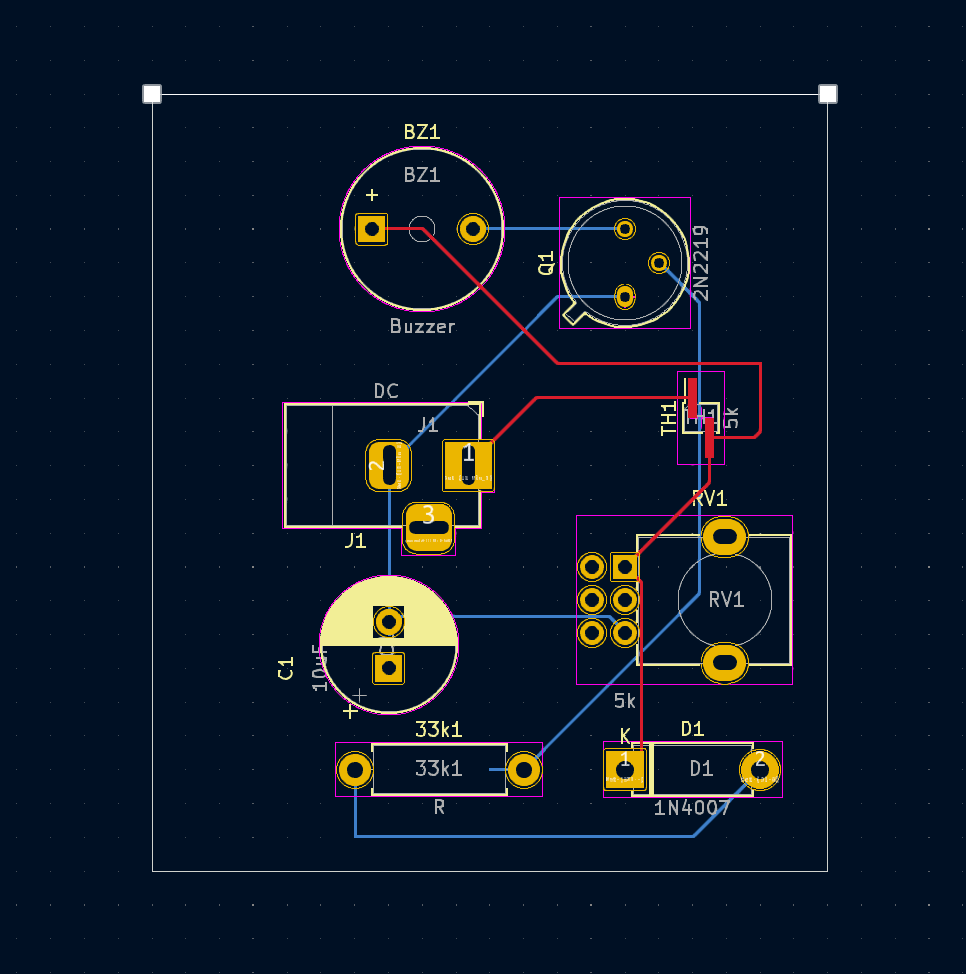 circuit with edge cuts
- You can view it in 3D, found in the drop-down view menu
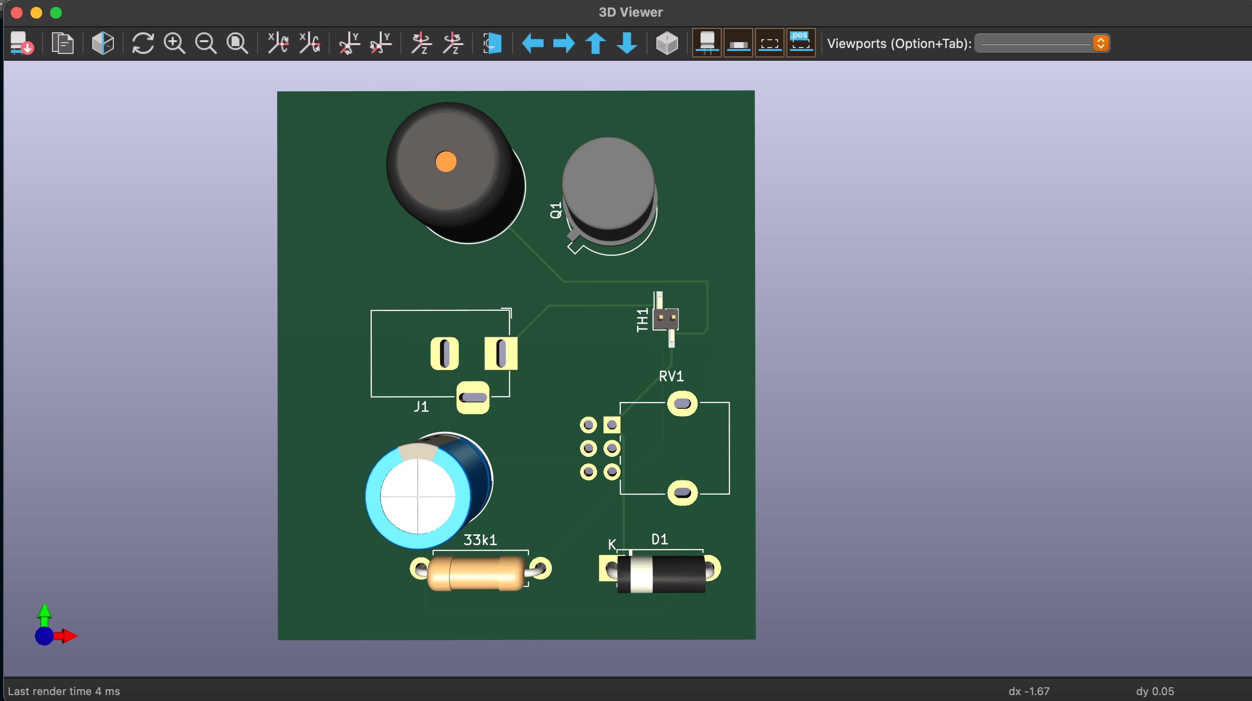 circuit in 3D view
-
To add mounting holes, select add footprint
- click on a part on the board that is empty and a pop-up window will appear
- find mounting hole, and the size you want (3.2mm M3 was used in tutorial)
- apply where you require them
-
Make sure all the yellow text (labels that will be printed) are confined within the board edge cuts
- You can add more text, like the title of your PCB
- there is a tool in the right toolbar
- a pop up window will appear where you can write the text
- select the same material as the rest of the text labels (F.Silkscreen)
- select the front copper layer
- To add filled zones, select the add a filled zone tool
- in the pop-up window, select a net to ground to????
-
select the edges of your board
- select the back copper layer
- add fill zone
- in the pop-up window, select a net to ground to???
-
select the edges of your board
- to export;
- click on plot in the top right bar
- in the pop-up window, select an output directory
- make sure front copper, back copper, front mask, back mask, front silk, back silk, and edge cut are selected
- click on plot
- click on generate drill file
SHORTCUTS:
m : hovering over a component and pressing key m to move it around
r : hovering over a component and pressing key r to rotate
command c : hovering over a component and pressing key c to copy it